Theoretical preliminary work and practical implementation
Based on the research activities in the first two years, the next step was to characterize the power components with focus on their high-frequency behavior and to optimize the structure of the laser driver stage. An important parameter, the parasitic inductance of the power loop on the PCB, was reduced by building it as compact as possible on a board with very thin layers. By measuring this parameter, it was possible to define the theoretical limits of what was feasible, thereby providing evidence for the optimal design of the system. This theoretical preliminary work enabled the researchers to further develop the previous multi-board solution into a single-board solution capable of generating pulses in the subnanosecond domain.
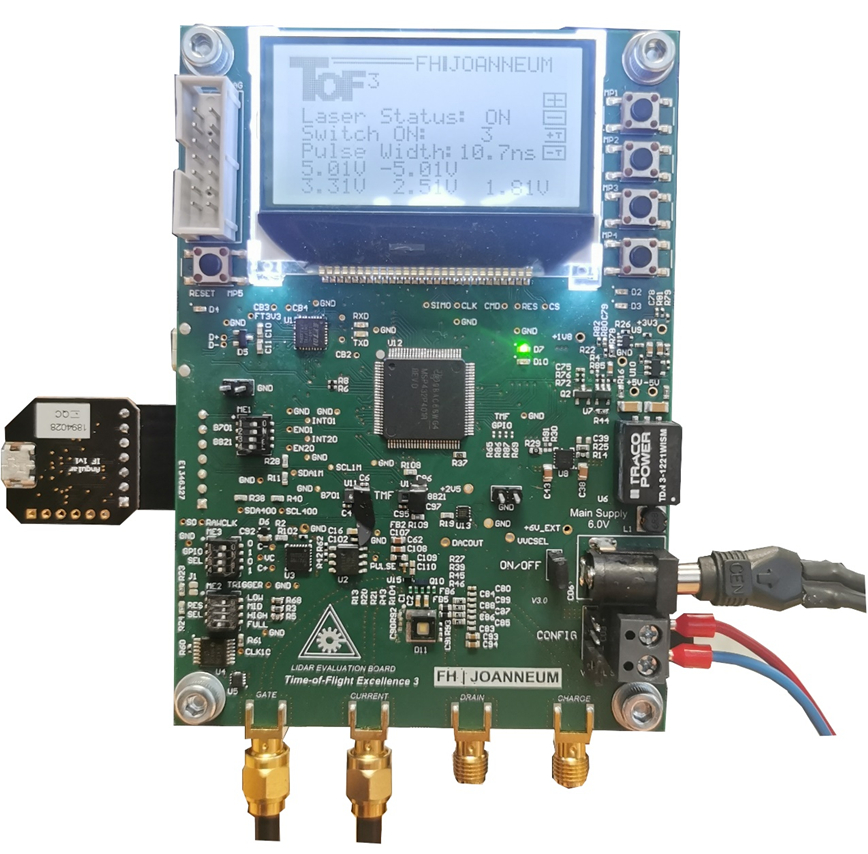
Demonstrator setup
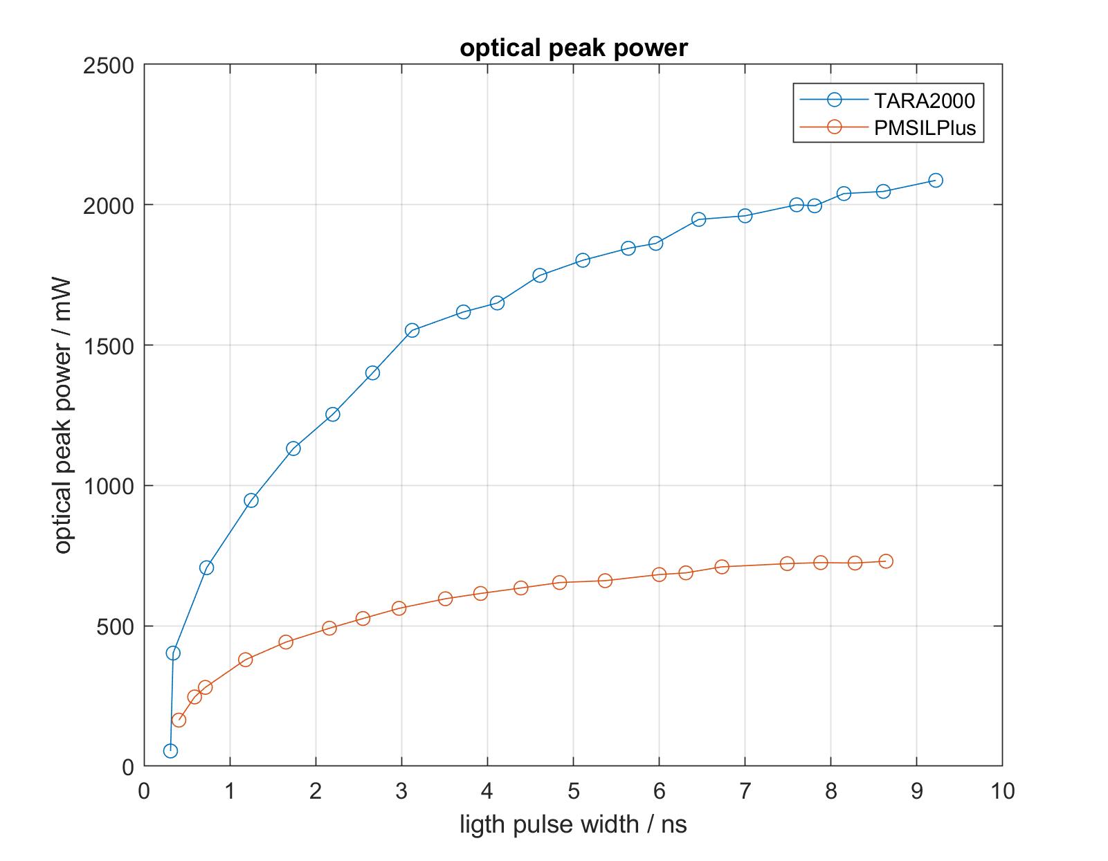
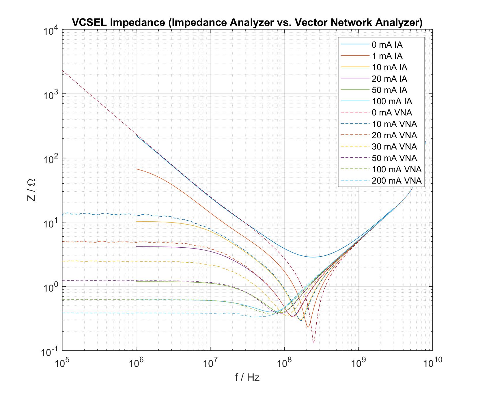
The board is equipped with two integrated lidar chips from ams OSRAM, of which one can be selected as an infrared receiver. A powerful VCSEL (vertical-cavity surface-emitting laser), which acts as an infrared transmitter. These infrared laser diodes with 940nm wavelength and an output power up to 2500mW increase the range of these lidar chips many times over. Because of the extremely short light pulses – in the range of 300ps to 10ns – all components of the transmitter power section were measured and simulated with respect to their high-frequency properties in the range from 100 kHz to 8 GHz. The main question was whether such short switching times can be achieved with the available components, and if so, whether the radiated light power and thus the achievable range would not be drastically reduced. Another question was the influence of parasitic effects that result from the structure of the electrical connections and component geometries on the PCB.


